BF979 Silicon PNP Planar RF Transistor
BF979 Silicon PNP Planar RF Transistor
BF979 Silicon PNP Planar RF Transistor

You also want an ePaper? Increase the reach of your titles
YUMPU automatically turns print PDFs into web optimized ePapers that Google loves.
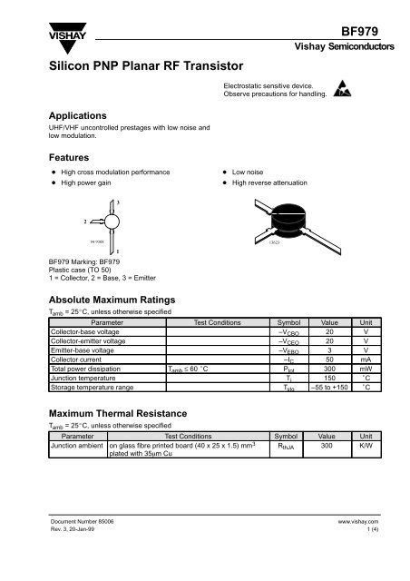
<strong>Silicon</strong> <strong>PNP</strong> <strong>Planar</strong> <strong>RF</strong> <strong>Transistor</strong><strong>BF979</strong>Vishay SemiconductorsElectrostatic sensitive device.Observe precautions for handling.ApplicationsUHF/VHF uncontrolled prestages with low noise andlow modulation.FeaturesHigh cross modulation performanceHigh power gainLow noiseHigh reverse attenuation3294 93081<strong>BF979</strong> Marking: <strong>BF979</strong>Plastic case (TO 50)1 = Collector, 2 = Base, 3 = Emitter13623Absolute Maximum RatingsT amb = 25 C, unless otherwise specifiedParameter Test Conditions Symbol Value UnitCollector-base voltage –V CBO 20 VCollector-emitter voltage –V CEO 20 VEmitter-base voltage –V EBO 3 VCollector current –I C 50 mATotal power dissipation T amb ≤ 60 C P tot 300 mWJunction temperature T j 150 CStorage temperature range T stg –55 to +150 CMaximum Thermal ResistanceT amb = 25 C, unless otherwise specifiedParameter Test Conditions Symbol Value UnitJunction ambient on glass fibre printed board (40 x 25 x 1.5) mm 3plated with 35m CuR thJA 300 K/WDocument Number 85006www.vishay.comRev. 3, 20-Jan-99 1 (4)
<strong>BF979</strong>Vishay SemiconductorsElectrical DC CharacteristicsT amb = 25 C, unless otherwise specifiedParameter Test Conditions Symbol Min Typ Max UnitCollector cut-off current –V CE = 20 V, V BE = 0 –I CES 100 ACollector-base cut-off current –V CB = 15 V, I E = 0 –I CBO 100 nAEmitter-base cut-off current –V EB = 3 V, I C = 0 –I EBO 10 ACollector-emitter breakdown voltage –I C = 1 mA, I B = 0 –V (BR)CEO 20 VDC forward current transfer ratio –V CE = 10 V, –I C = 10 mA h FE 20 50 90Electrical AC CharacteristicsT amb = 25 C, unless otherwise specifiedParameter Test Conditions SymbolMin Typ Max UnitTransition frequency –V CE = 10 V, –I C = 10 mA, f = 300 MHz f T 1750 MHzTransition frequency –V CE = 10 V, –I C = 30 mA, f = 300 MHz f T 1300 MHzCollector-base capacitance –V CB = 10 V, f = 1 MHz C cb 0.6 pFNoise figure –V CE = 10 V, –I C = 10 mA, Z S = 50 , F 3.4 4.2 dBf = 800 MHzPower gain–V CE = 10 V, –I C = 10 mA, Z S = 50 , Z L G pb 16 dB= 500 f = 800 MHzCollector current for G pbmax –V CE = 10 V, Z L = 500 f = 800 MHz –I C 10 mATypical Characteristics (T amb = 25 C unless otherwise specified)P tot – Total Power Dissipation ( mW )128454003503002502001501005000 20 40 60 80 100 120 140 160T amb – Ambient Temperature ( °C )Figure 1. Total Power Dissipation vs.Ambient Temperaturef – Transition Frequency ( MHz )T128482100180015001200900600300–V CB =10Vf=300MHz00 5 10 15 20 25 30 35–I C – Collector Current ( mA )Figure 2. Transition Frequency vs. Collector Currentwww.vishay.com2 (4)Document Number 85006Rev. 3, 20-Jan-99
IdeasAnimal welfare definition and methodology - livestock (including aquaculture species of fish, crustacea)Evaluation of welfare outcomes of new Livestock Transport StandardsHumane alternatives to high risk husbandry procedures - castration, dehorning, tail docking mulesing (includes research of public attitudes andeducation methods)Humane loading and unloading of bobby calves - evaluation of methods,operator/processor attitude survey, education development, evaluationIntensive housing design for good welfare for sheep & pregnant sowsN or CO2 Foam depopulation technique for humane mass destructionPortable mass destruction methods for livestock - maceration, electrocution, gassing system evaluationResearch consumer attitudes to welfare and labelling.Research free range economics and training programsResearch group housing of sows welfare outcomesResearch long distance transport welfare affects on poultry, pigs, cattle (pregnant cattle and bobby calves) and sheepStockperson training program - research on education methods and stakeholder attitudesSurvey of layer hen cage types and assessment of welfare outcomesTraining program for welfare inspectors - police, councils, RSPCA, DPIWelfare methodology for defined (POCTA) species used in aquaculture – incl’ slaughter methods, disposal of ornamental species, pet shopstandardsField evaluation of Lethal Trap Devices and Tranquiliser Trap DevicesEvaluation of trap pan tension settings to improve species sensitivity.
<strong>BF979</strong>Vishay SemiconductorsOzone Depleting Substances Policy StatementIt is the policy of Vishay Semiconductor GmbH to1. Meet all present and future national and international statutory requirements.2. Regularly and continuously improve the performance of our products, processes, distribution and operatingsystems with respect to their impact on the health and safety of our employees and the public, as well as theirimpact on the environment.It is particular concern to control or eliminate releases of those substances into the atmosphere which are known asozone depleting substances (ODSs).The Montreal Protocol (1987) and its London Amendments (1990) intend to severely restrict the use of ODSs andforbid their use within the next ten years. Various national and international initiatives are pressing for an earlier banon these substances.Vishay Semiconductor GmbH has been able to use its policy of continuous improvements to eliminate the use ofODSs listed in the following documents.1. Annex A, B and list of transitional substances of the Montreal Protocol and the London Amendments respectively2. Class I and II ozone depleting substances in the Clean Air Act Amendments of 1990 by the EnvironmentalProtection Agency (EPA) in the USA3. Council Decision 88/540/EEC and 91/690/EEC Annex A, B and C (transitional substances) respectively.Vishay Semiconductor GmbH can certify that our semiconductors are not manufactured with ozone depletingsubstances and do not contain such substances.We reserve the right to make changes to improve technical design and may do so without further notice.Parameters can vary in different applications. All operating parameters must be validated for each customer applicationby the customer. Should the buyer use Vishay-Semiconductors products for any unintended or unauthorized application, thebuyer shall indemnify Vishay-Semiconductors against all claims, costs, damages, and expenses, arising out of, directly orindirectly, any claim of personal damage, injury or death associated with such unintended or unauthorized use.Vishay Semiconductor GmbH, P.O.B. 3535, D-74025 Heilbronn, GermanyTelephone: 49 (0)7131 67 2831, Fax number: 49 (0)7131 67 2423www.vishay.com4 (4)Document Number 85006Rev. 3, 20-Jan-99